SWIR Cameras for Semiconductor Inspection

Revolutionizing Semiconductor Inspection with Advanced SWIR Camera Technology
The Critical Need for Precision Inspection
Semiconductor manufacturing demands flawless quality control systems. Optical inspection must detect both surface and hidden defects in wafers and components. Undetected flaws can compromise electrical performance and structural integrity. Therefore, advanced inspection technology becomes essential for maintaining quality standards.
SWIR Technology Advantages
Short Wavelength Infra-Red cameras offer unique inspection capabilities. Silicon transparency at 1,100 nm wavelengths enables subsurface visualization. Consequently, manufacturers can identify internal cracks and impurities invisible to standard vision systems. This technology significantly enhances defect detection accuracy.
Semiconductor Market Context
Integrated circuits form the foundation of modern electronic devices. Global semiconductor sales continue growing exponentially, particularly for AI applications. Manufacturing defects create substantial financial impacts across supply chains. Thus, reliable inspection systems provide crucial protection against costly production errors.
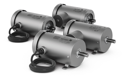
SVS-Vistek Technical Solutions
SVS-Vistek’s SenSWIR FXO cameras deliver up to 5.2 megapixel resolution for precise inspection. The extended wavelength range covers both visible and SWIR spectra simultaneously. This eliminates the requirement for multiple camera setups. Moreover, high-speed interfaces support rapid frame rates for efficient processing.
Camera Performance Features
The SenSWIR series combines high resolution with exceptional frame rates. Advanced thermal management ensures consistent image quality and dynamic range. Additionally, integrated strobe controllers support complex illumination scenarios. These features collectively enhance inspection accuracy and reliability.
Integration and Cooling Innovations
GenICam 3.0 compatibility simplifies software integration processes. The recently added thermoelectric cooling option reduces sensor noise significantly. This Peltier-effect cooling improves image quality by minimizing thermal interference. Therefore, manufacturers achieve superior defect detection capabilities.
Industry Application Benefits
Semiconductor foundries implementing this technology experience improved production yields. The ability to detect subsurface defects prevents downstream quality issues. Furthermore, streamlined integration reduces implementation complexity and costs. These advantages make SWIR inspection increasingly valuable for modern fabrication facilities.
Technical Implementation Strategy
Manufacturers should prioritize critical inspection points where subsurface defects cause significant impacts. The simultaneous visible and SWIR imaging capability simplifies system architecture. Additionally, high-speed interfaces maintain throughput while enhancing inspection quality. This balanced approach optimizes both performance and efficiency.
Frequently Asked Questions
How does SWIR technology detect subsurface defects?
Silicon’s transparency at SWIR wavelengths allows cameras to visualize internal structures and hidden flaws invisible to conventional vision systems.
What resolution do SVS-Vistek SWIR cameras provide?
The SenSWIR FXO series offers resolutions up to 5.2 megapixels with high frame rates for detailed inspection.
Why is thermoelectric cooling important for these cameras?
TEC reduces thermal noise and dark current, significantly improving image quality for precise defect detection.
Can these cameras replace multiple inspection systems?
Yes, the extended wavelength range enables simultaneous visible and SWIR imaging, eliminating need for separate camera setups.
What interfaces support high-speed data transfer?
10GigE Vision and CoaXPress CXP-12 interfaces maintain maximum frame rates for efficient inspection processes.


LEAVE A COMMENT